INFORMATIONAL ADVISORY REGARDING PCBs PRESENT IN
SEALANTS AND PAINTS IN OLDER BUILDINGS

Caulking around window containing PCBs
During repair
and restoration work after flood events, such as the damages caused by Hurricane
Irene and Superstorm Sandy, the workers had to deal with older sealants (pre
1979) installed around doors, windows, chimneys, etc. In the projects where we were involved, we
advised the insureds of the potential presence of PCBs in the sealants and
roofing materials in the older buildings.
The old fluorescent light balasts are also a source of PCBs. PCBs have been detected in caulk in
buildings, including schools, with concentrations ranging from as low as 50 ppm
to as high as 440,000 ppm. In many
cases, PCBs were used in caulk with a concentration as high as 30%. We
provide this industry-wide informative advisory regarding the potential for
sealants located in exterior walls of buildings to contain polychlorinated
biphenyls (PCBs) at levels that warrant certain measures.
A.
BACKGROUND
PCBs were a
common additive to sealants because of their water and chemical resistance,
durability, and elasticity. PCBs were
added as a plasticizer in sealants used primarily to seal joints between
masonry units and around windows. Other
areas where PCBs have been found include:
Building Materials
•
Caulking, Paints, Sealants used in
waterproofing, anti-fouling, and as fire retardants
•
Roofing Materials
•
Expansion Joints
•
Adhesives
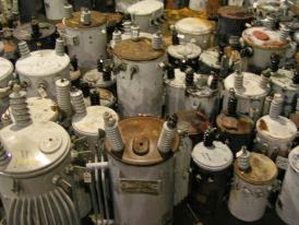
Industrial Applications
•
Capacitors, Transformers
•
Fluorescent Ballasts
•
Machinery, Furnaces
•
Masonry Walls
Sealants
containing PCBs were employed in some buildings, including schools, primarily
between 1950 and 1980. PCBs were also
used in other building materials such as paints, mastics, adhesives, and
specialty coatings. Although the use of
sealants containing PCBs has long since been prohibited, these types of
sealants may still be present in existing buildings where new sealants were
applied over the top of the existing sealant or where general lack of long-term
maintenance has not addressed the existing conditions.
PCBs belong to a
broad family of man-made organic chemicals known as chlorinated hydrocarbons. Due to their nonflammability, chemical
stability, high boiling point, and electrical insulating properties, PCBs were
used in hundreds of industrial and commercial applications, including
electrical, heat transfer, and hydraulic equipment; and as plasticizers in
paints, plastics, rubber products, and building caulk. PCBs were manufactured domestically starting
in 1929, until they were banned from manufacture in 1979.
Exposure to PCBs
can cause a variety of adverse health effects in animals and humans. In animal studies, PCBs have been shown to
cause cancer as well as serious noncancer health effects. In humans, PCBs are potentially cancer-causing
and can cause other noncancer effects, including immune system suppression,
liver damage, endocrine disruption, and damage to the reproductive and nervous
systems.

PCB-containing
mastic used to seal the front and back shields
B.
RISKS
The potential
risks identified by the U.S. Environmental Protection Agency (EPA) include
touching or inhaling dust produced from a deteriorating PCB-containing sealant.
Potential exposure may also occur by
individuals who practice maintenance and/or repairs on buildings that involve
the routine replacement of building sealants. The EPA also indicates that PCBs may leach
into building materials such as wood, masonry, etc. that are in direct contact
with the PCB-containing sealant.

C.
DISCUSSION
Renovation or
restoration projects on existing buildings often include the replacement of
deteriorated sealants in joints located on the exterior skin of the building. The designers and contractors involved in such
projects should be aware of the potential for PCBs in existing sealants, as
disturbance of these sealants may result in contamination of adjacent interior
and exterior areas. At this time, the
EPA has not required widespread sampling and testing of public and commercial
buildings. The EPA has, however,
established guidelines for testing of sealants and testing of interior air for
PCBs. These guidelines can be found
online at http://www.epa.gov/pcbsincaulk/guide/guide-sect3.htm.
Since PCB
release can result in public health hazards, it is recommended that owners,
contractors, and designers involved in renovation projects on older buildings
retain qualified hazardous materials consultants to determine the presence of
PCBs in sealants and to develop an appropriate remediation response. Not only should the actual sealant be tested
for PCBs, but adjacent building materials (e.g., brick, cinder block, or wood)
should also be tested, as PCBs in sealant can migrate into surrounding
material.
For determining the presence of PCBs in indoor air, EPA has two
approved methods: Compendium of Methods for the Determination of Toxic
Organic Compounds in Ambient Air – Compendium Method TO-4A (high-air volume)
and Compendium Method TO-10A (low-air volume).

D. ISSUES
The possible issues to consider include the following:
·
Potential for worker and
public exposure to PCBs as the result of disturbance of the sealant
·
Potential for PCB
contamination of interior and exterior areas adjacent to subject work areas
·
Potential for PCB
contamination of surrounding building materials
PCBs
– A Question of Due Diligence
The
use of polychlorinated biphenyls (PCBs) was widespread before 1977, and the
health risks associated with PCBs are well known. PCBs have been widely studied, analyzed,
regulated, and managed since the Toxic Substances Control Act (TSCA) was passed
in 1976. Over the nearly four decades
since 1977, PCBs have been found in a wide variety of building products,
including sidewalk caulk, window glazing, expansion joints, crack sealants,
caulks used as gaskets, surface coatings (e.g. paint), and caulks used between
masonry blocks, among other uses. Much of this material still remains in
excellent condition, and largely as it was the day that it was installed. This
remarkable durability of PCB caulks is a testament to the physical and chemical
properties of PCBs!
EPA
has studied PCBs in caulk (including surface coatings), investigated PCB caulk
in school buildings, and developed regulations and guidelines for PCBs in caulk
when discovered. However, EPA does not require commercial landowners, States,
or municipalities to test for the presence of PCBs in caulk. PCBs are only
regulated in caulk and building materials contaminated by caulk when
discovered. In some instances, municipalities, private lenders, and public
lending agencies require testing for PCBs in caulk. However, there still
remains no Federal requirement to do so.
PCBs
in caulk are a problem from both public health and landowner perspectives. From
a public health perspective, the health risks of PCBs themselves are well
known, and the presence of PCBs in caulk have been found to create significant
human and ecological exposures. However, the risk of PCBs in caulk in the built
environment has not been fully quantified. In addition, the scope of the
problem -the amount of affected caulk that is out there – is entirely unknown.
What
This Means To The CRE Industry
For
a commercial landowner or prospective purchaser…“when discovered”…presents a
problem. Should PCBs in caulk (>50 ppm PCBs) be discovered, the caulk is not
an approved use under TSCA, and the caulk has to be removed as a PCB bulk
product waste (40 CFR Part 761.62). Porous surfaces such as masonry that are
contaminated may continue to remain in use for the useful life of the
material as long as encapsulated using the methods required under 40 CFR Part
761.61. Such a task is neither simple nor inexpensive, and can require a small
army of environmental consultants, attorneys, and contractors to complete. When
purchasing an older commercial building, the purchaser has a voluntary decision
to make during due diligence: to perform a PCB Caulk Assessment or
not (health concerns aside).
Since
there is no obligation to test for PCB caulks (other than to provide a safe
environment for building occupants), the purchaser or landowner may never have
to identify, manage or dispose of PCB caulk and affected porous surfaces. As a
result, its presence could result in no financial exposure if never discovered.
On
the other hand, if PCBs are discovered after closing or during
demolition/reconstruction, PCB caulk could create a significant regulatory
requirement to remove the caulk and manage affected materials in the middle of
a demolition or renovation project. Even worse, PCBs could be discovered after
a renovation has been completed, necessitating remediation of a newly finished
space. Such scenarios have far reaching implications. Discovering caulk
“after the fact” can have dire consequences. The potential for an unexpected
cost exposure can have a big impact on budgets, schedules, and asset values.
The not insignificant cost of dealing with PCB caulk can disrupt financing, and
wreak all manner of havoc with respect to third party liability, insurance,
building occupants, and regulatory compliance.
Even
if not discovered during ownership, a new prospective purchaser may perform a
PCB Caulk Assessment during future due diligence, develop a remediation
estimate, and demand a purchase price reduction to pay for the cost of its
management and disposal. If the deal falls apart, the presence of PCB caulk is
then a known condition that needs to be disclosed to the next buyer,
potentially devaluing the asset. In addition, a known condition may not be
insurable.
The
issue of PCBs in caulk will not go away. The problem is that these caulking
materials could be anywhere in the United States, they slowly dust and off-gas
into the indoor environment, leach over time to adjacent masonry, other
surfaces, and even to soil, sediment, and storm water. PCBs from caulk have
also been found at significant concentrations in indoor air. If PCBs that have
leached from caulk are found in soil, the soil should then be regulated as a
PCB remediation waste (40 CFR Part 761.61).

At
the present time, the EPA has not adopted an approach to require testing PCBs
in caulk. Even if a requirement to test caulk for PCBs emerged, the regulators
don’t have the resources or personnel to manage the large volume of work plans,
reviews, and approvals necessary to manage the issue. Since TSCA is a Federal
regulation, states and municipalities don’t have the authority to make
decisions for the EPA. Such a regulatory log jam on the Federal level is
unthinkable.
The
decision to test or not test for PCBs in caulk belongs to the purchaser during
due diligence. The risks of not
testing include 1) buying a building with a hidden health hazard,
and 2) buying a building with a hidden financial liability…often a big
liability. The risk of testing
includes incurring a significant expense now that may never otherwise come to
fruition because PCBs may never be identified. Given that this caulk is not
painted bright red to signify its presence, it represents an invisible
potential health hazard and financial liability.
For
the EPA, the issue of PCBs in caulk is the classic hot potato: the scope of the
problem is unknown, may be vast, and there may not be a cost effective and
logistical way to deal with what may or may not be a significant public health
issue. PCBs in caulk are an emerging issue. Should you chose to avoid it, the
likelihood that PCBs will be discovered at some point by a contractor,
employee, or other party is ever increasing. So, you are on your own. Given
this framework, you can seek opinions, but the decision is yours to make.
EPA Advisory: PCBs in Caulk in Older Buildings
Overview
In recent years, EPA
has learned that caulk containing potentially harmful polychlorinated
biphenyls (PCBs) was used in many buildings, including schools, in the
1950s through the 1970s. Most schools and buildings built after 1979 do not
contain PCBs in caulk. On September 25, 2009, EPA announced new guidance for
school administrators and building managers with important information about
managing PCBs in caulk and tools to help minimize possible exposure. Through EPA PCB
Regional Coordinators, the Agency will also assist communities in
identifying potential problems and, if necessary, developing plans for PCB
testing and removal.
For more information:
·
PCBs in Caulk Fact Sheet
(PDF) (2 pp, 26 KB)
·
PCBs In Caulk Frequent
Questions (PDF) (14 pp, 101 KB)
The EPA is conducting
research to address several unresolved scientific questions that must be better
understood to assess the magnitude of the problem of PCBs in caulk and identify
the best long-term solutions. For example, the link between the concentrations
of PCBs in caulk and PCBs in the air or dust is not well understood. The Agency
is doing research to determine the sources and levels of PCBs in schools and to
evaluate different strategies to reduce exposures. The results of this research
will be used to provide further guidance to schools and building owners as they
develop and implement long-term solutions. Read more about Research on PCBs in
Caulk.
EPA has calculated
prudent public health levels that maintain PCB exposures below the “reference
dose” – the amount of PCB exposure that EPA does not believe will cause harm.
Read Public
Health Levels for PCBs in Indoor School Air || PDF
version (2 pp, 14 KB)

Background
Caulk is a flexible
material used to seal gaps to make windows, door frames, masonry and joints in
buildings and other structures watertight or airtight. At one time caulk was
manufactured to contain PCBs because PCBs imparted flexibility.
First Step: Take
Steps to Minimize Exposure
Although this is a
serious issue, the potential presence of PCBs in schools and buildings should
not be a cause for alarm. If your school or building was built or renovated
between 1950 and 1979, there are several steps schools can take to reduce
potential exposure until it can be determined with certainty if PCBs are
present in caulk used in the building and any contaminated caulk can be
removed. One of the most important steps is to minimize the potential for PCBs
to be present in the indoor air. Indoor air levels of PCBs within a school can
be reduced by ensuring that the ventilation system is operating as designed,
and to repair or improve the system if it is not.
Many old lighting
systems contain ballasts manufactured with PCBs. These PCBs can get into the
air if the ballast fails or ruptures. Replacement of old lighting systems with
new, energy efficient systems will eliminate a potential source of PCBs.
Other steps include:
·
Clean
frequently to reduce dust and residue inside buildings.
·
Use
a wet or damp cloth or mop to clean surfaces.
·
Use
vacuums with high-efficiency particulate air (HEPA) filters.
·
Do
not sweep with dry brooms; minimize the use of dusters.
·
Wash
children's hands with soap and water often, particularly before eating.
·
Wash
children's toys often.
·
Wash
hands with soap and water after cleaning, and before eating or drinking.
EPA also has
developed an informational brochure to provide the general public with
important information on PCBs in building caulk, Preventing Exposure to
PCBs in Caulking Material || PDF version (4
pp, 2.7 MB) || en
Español (PDF) (4 pp, 2.7 MB), EPA Publication EPA-747-F-09-005.

Testing
Air
If school
administrators and building owners are concerned about potential PCBs in the
caulk, they should consider testing to determine
if PCBs are present in the air. If testing reveals PCB levels above the levels
EPA has determined to be safe, schools should attempt to identify any potential
sources of PCBs that may be present in the building, including testing samples
of caulk and looking for other potential PCB sources (e.g., old transformers,
capacitors, or fluorescent light ballasts that might still be present at the
school).
If elevated levels of
PCBs are found in the air, schools should also have the ventilation system
evaluated to determine if it is contaminated with PCBs. Although the
ventilation system is unlikely to be an original source of PCB contamination,
it may have been contaminated before other sources of PCBs were removed from
the school and may contribute to elevated air levels of PCBs. Contaminated
ventilation systems should be carefully cleaned. Ideally, such cleaning
should be planned in concert with removal of any sources of PCBs that are found
to avoid re-contamination of the system.
During the search for
potential sources, schools should be especially vigilant in implementing
practices to minimize exposures and should retest to determine whether those
practices are reducing PCB air levels. It is important to note that interior
surfaces and settled dust can absorb PCBs from contaminated air, and these
“secondary sources” can emit PCBs after the primary source is removed.
Therefore, a remediation plan should consider the potential effects for these
secondary sources on indoor air quality.
Other Sources,
Including Caulk
Should those
practices not reduce exposure, caulk and other known sources of PCBs (e.g.,
paints, floor and ceiling tiles) should be removed as soon as practicable.
Please note that you cannot tell if caulk has PCBs by looking at it. While it
is possible that PCBs could be released into the environment through the
cracking or flaking of caulk, EPA believes the old caulk that is still flexible
or is in visibly good condition could be a significant source of PCBs into the
air. The only way to be sure that caulk has PCBs is to have a professional test
the caulk.
Where schools or
other buildings were constructed or renovated between 1950 and 1979, EPA
recommends that PCB-containing caulk be removed during planned renovations and
repairs (when replacing windows, doors, roofs, ventilation, etc.).
Based on EPA's Office
of Research and Development's (ORD) laboratory research, encapsulation was
found to be most effective for interior surfaces that contain low levels of
PCBs (i.e. several hundred parts per million). Depending on the PCB reduction
goal, the performance of the encapsulant, and the conditions of the building,
the upper limit of the PCB concentration for successful encapsulation may vary.
Therefore, post-encapsulation monitoring is an essential part of the
encapsulation process. Building owners should consult EPA's research
on this issue for more specifics. Encapsulation may be useful for the reduction
of emissions from secondary sources such as contaminated building materials
under and around PCB-containing caulk or paint that has been removed.
Encapsulation was not found to be effective in reducing emissions from sources
that have a high PCB content (for example caulk) for more than a short period
of time. Because each site will present unique circumstances, please consult
your EPA
PCB Regional Coordinator regarding the application of encapsulation
measures on a case by case basis. It is critically important to assure that
PCBs are not released to air during replacement or repair of caulk in affected
buildings. Assessment of the ventilation system for potential
contamination, proper cleaning when required, and isolation of the system to
prevent further contamination are also important.

Test Methods
For determining the
presence of PCBs in indoor air, EPA has two approved methods:
• Compendium
of Methods for the Determination of Toxic Organic Compounds in Ambient Air -
Compendium Method TO-4A (high air volume) (PDF) (53 pp, 665 KB)
• Compendium
of Methods for the Determination of Toxic Organic Compounds in Ambient Air -
Compendium Method TO-10A (low air volume) (PDF) (37 pp, 288 KB)
.
EPA recommends that
caulk suspected to contain PCBs be tested directly for the presence of PCBs and
removed if PCBs are present at significant levels. The PCB regulations provide
appropriate methods for testing. More information on these procedures can be
found at:
• Wipe
Sampling (PDF) (31 pp, 86K)
Contact EPA's Toxic
Substances Control Act (TSCA) Hotline at 1-888-835-5372 or the EPA PCB
Regional Coordinator for your state for assistance.
Schools Information
Kit
A Schools Information
Kit provides information for parents, students and staff about PCBs in
caulk, including:
• General
information on PCBs in older schools and buildings || PDF version (1
pg, 564 KB) || en
Español (PDF) (1 pg, 517 KB)
• Schools
checklist || PDF
version (1 pg, 416 KB) || en Español (PDF)
(1 pg, 221 KB)
Information for
Contractors Working in Older Buildings
Read Contractors Handling
PCBs in Caulk During Renovation, EPA's guidance to contractors and
maintenance personnel working in older buildings that may contain
PCB-contaminated caulk.
Additional
Information
Additional EPA
brochures and fact sheets on best practices for addressing PCBs in caulk:
· Fact Sheet: Removal and
Clean-Up of PCBs in Caulk and PCB-Contaminated Soil and Building Materials
Where Can I Get More
Information?
For more information
on how to properly test for and address PCBs in caulk, call the EPA's Toxic
Substances Control Act (TSCA) Hotline at 1-888-835-5372 or contact the EPA PCB
Regional Coordinator for your state.

EPA Fact Sheet - PCBs in Caulk
PCBs
•
Polychlorinated biphenyls (PCBs) are
man-made chemicals that persist in the environment and were widely used in
construction materials and electrical products prior to 1979.
•
PCBs can affect the immune system,
reproductive system, nervous system and endocrine system and are potentially
cancer-causing if they build up in the body over long periods of time.
•
Congress banned manufacture and use of
PCBs in 1976 and they were phased out in 1979 except in certain limited uses.
PCBs in Caulk
•
PCBs may be present in the caulk used
in windows, door frames, and masonry columns, and other building materials in
many schools and other buildings built or renovated between 1950 and 1979.
•
In some cases, PCBs represent a high
percentage of the caulk, e.g. 100,000 parts per million (ppm) or higher.
•
Because PCBs can migrate from the caulk
into air, dust, surrounding materials and soil, EPA is concerned about
potential PCB exposure to school children and other building occupants.
•
The link between PCBs in caulk and
exposures to PCBs in the air or dust is not well understood. EPA has conducted research to better
understand the link between PCBs in caulk and exposures to PCBs in the air and
in dust.
•
People are exposed to PCBs from many
sources, including diet, but air or dust levels in buildings may account for a
significant portion of exposure.
•
The air levels of PCBs to which
individuals may be exposed vary depending on the age of the person exposed and
the amount of time the person spends in building areas where PCBs are present.
EPA has calculated prudent public health levels that maintain PCB exposures
below the “reference dose” – the amount of PCB exposure that EPA does not believe
will cause harm. Those levels vary depending on the age group and use
assumptions about potential PCB exposures in schools and from other sources,
such as diet.

Immediate Steps to Reduce Exposure
•
Though this is a serious issue, the
potential presence of PCBs in schools and buildings should not be a cause for
alarm – there are steps school administrators and building owners can take to
protect students, teachers and others.
•
One important step that a school system
can do is to minimize the potential for PCBs to be present in the indoor air.
Indoor air levels of PCBs within a school can be reduced by ensuring that the
ventilation system is operating as designed, and to repair or improve the
system if it is not.
EPA recommends
the following “best practices” to minimize potential exposure:
o
Clean frequently to reduce dust and
residue inside buildings
o
Use a wet or damp cloth or mop to clean
surfaces
o
Using vacuums with high efficiency
particulate air filters
o
Do not sweep with dry brooms; minimize
the use of dusters
o
Wash children’s hands with soap and
water often, particularly before eating
o
Wash children’s toys frequently
o
Wash hands with soap and water after
cleaning, and before eating or drinking.

Testing the Air for PCBs and Addressing Elevated Levels
• If school administrators and building owners are concerned
about exposure to PCBs and wish to supplement these steps, EPA recommends
testing to determine if PCB levels in the air exceed EPA’s suggested public
health levels.
• Schools should attempt to identify any potential sources of
PCBs that may be present in the building, including testing samples of caulk
and looking for other potential PCB sources (e.g., old transformers,
capacitors, or fluorescent light ballasts that might still be present at the
school). While it is possible that PCBs could be released into the environment
through the cracking or flaking of caulk, EPA believes the old caulk that is
still flexible or is in visibly good condition could be a significant source of
PCBs into the air. The only way to be sure that caulk has PCBs is to have a
professional test the caulk.
• If elevated air levels of PCBs are found, schools should
have the ventilation system evaluated to determine if it is contaminated with
PCBs. Although the ventilation system is unlikely to be an original source of
PCB contamination, it may have been contaminated before other sources of PCBs
were removed from the school and may be contributing to elevated air levels.
Contaminated ventilation systems should be carefully cleaned. Ideally, such
cleaning should be planned in concert with removal of any sources of PCBs that
are found to avoid re-contamination of the system.
• During the search for potential sources, schools should be
especially vigilant in implementing to minimize exposures and should retest to
determine whether those practices are reducing PCB air levels.
• If these measures do not reduce exposures, caulk and other
known sources of PCBs should be removed as soon as practicable.

Removal of PCB-contaminated Caulk
during Renovations and Repairs
• Where schools or other buildings were constructed or
renovated between 1950 and 1979, EPA recommends that PCB-containing caulk be
removed during planned renovations and repairs (when replacing windows, doors,
roofs, ventilation, etc.)
• It is critically important to ensure that PCBs are not
released into the air during renovation or repair of affected buildings. EPA is
recommending simple, common sense work practices to prevent the release of PCBs
during these operations.
• Assessment of the ventilation system for potential
contamination, proper cleaning when required, and isolation of the system to
prevent further contamination are also important.
• A list of these work practices can be found at www.epa.gov/pcbsincaulk
• Encapsulation of PCB-containing Caulk Based on EPA's Office
of Research and Development's laboratory research, encapsulation was found to
be most effective for interior surfaces that contain low levels of PCBs (i.e.
several hundred parts per million).
• Depending on the PCB reduction goal, the performance of the
encapsulant, and the conditions of the building, the upper limit of the PCB
concentration for successful encapsulation may vary.
• Therefore, post-encapsulation monitoring is an essential
part of the encapsulation process. Building owners should consult EPA's
research on this issue for more specifics (see ORD report).
• Encapsulation may be useful for the reduction of emissions
from secondary sources such as contaminated building materials under and around
PCB-containing caulk or paint that has been removed.
• Encapsulation was not found to be effective in reducing
emissions from sources that have a high PCB content (for example caulk) for
more than a short period of time.
• Because each site will present unique circumstances, please
consult your EPA PCB Regional Coordinator regarding the application of encapsulation measures on a
case by case basis.
EPA Research on PCBs in Buildings
• EPA has conducted research
to: 1) characterize potential sources
of PCB exposures in schools (caulk, coatings, light ballasts, etc.); 2)
investigate the relationship of these sources to PCB concentrations in air,
dust, and soil; and, 3) evaluate methods to reduce exposures to PCBs in caulk
and other sources.
• Read more about the results of this research.
For More Information
• Building owners and school administrators seeking additional
guidance and information can call the Toxic Substances Control Act (TSCA)
Hotline (888) 835-5372.
• Schools, parents, building owners and contractors can find
information on the safe handling and renovation of potentially contaminated
caulk here: www.epa.gov/pcbsincaulk

Contractors: Handling PCBs in Caulk During Renovation
This brochure is meant to provide
contractors, parents, teachers, and school administrators a general overview of
the practices a contractor should consider when conducting the renovation of a
building that has polychlorinated biphenyl (PCB)-containing caulk. PCBs were
not added to caulk after 1979. Therefore, in general, schools built after 1979
do not contain PCBs in caulk.
Contractors
play an important role in protecting public health by helping prevent exposure
to toxic PCBs. Ordinary renovation and maintenance activities involving the
removal of PCB-containing caulk and the surrounding contaminated substrate
(brick, masonry, cinder block, wood, etc.) can create dust that contains PCBs
which can expose children and adults. PCBs have been demonstrated to cause a
variety of adverse health effects, including cancer in animals. PCBs have also
been shown to cause a number of serious non-cancer health effects in animals,
including effects on the immune system, reproductive system, nervous system,
endocrine system, and other health effects.
Consider
Testing the Air in Buildings Built Between 1950 and 1979 to Determine Whether
Your School or Building May Have PCBs
If
school administrators and building owners are concerned about exposure to PCBs
and wish to supplement the steps recommended in this brochure, EPA recommends
testing to determine if PCB levels in the air exceed EPA's suggested public
health levels. If testing reveals levels above the suggested public health
levels, school and building operators should be especially vigilant in
implementing and monitoring practices to minimize exposures. If PCBs are found
in the air, EPA will assist in developing a plan to reduce exposure and manage
the caulk. You cannot tell if caulk has PCBs by looking at it. EPA
believes the old caulk that is still flexible or is in visibly good condition
may be a significant source of PCBs into the air. The only way to be sure
that caulk has PCBs is to have a professional test the caulk. Your EPA
Regional PCB Coordinator can direct you to a PCB testing lab.

- Be in compliance with occupational protection regulations for contractors (PDF) (2 pp, 286K).
- Protect building occupants and passersby by containing the work area to prevent PCB-containing caulk dust from getting into the surrounding environment.
- Determine disposal options based on concentration and type of material.
- Place an encapsulant underneath the new caulk/sealant (since PCBs in the adjoining material can move into the new caulk/sealant). Use replacement caulk/sealant that is free of environmental hazards.
A pilot renovation project may be warranted to verify whether the renovation goals can be met. It will allow you to compare methods, tools, and protective measures to get specific information about their effectiveness and cost.
Before Starting the Job, Consider the Types of Tools and Machinery for Removing Caulk
- Manual tools are recommended for soft flexible caulk:
- Advantages: no dust and no heat
- Disadvantages: labor intensive and slow
- Electromechanical tools are recommended for hardened/brittle caulk:
- Advantages: faster, less labor intensive
- Disadvantages: generate heat (which can volatilize the PCBs) and dust, requiring added protective measures. Also must consider the potential abrasive effects on sensitive adjoining structures (e.g., wood and metal).
- EPA recommends removing as much of the old caulk as possible, since any residual caulk left in place can contaminate any new caulk or sealant that is applied.

Notify Interested Parties and Plan for Emergencies
- Communicate the goals, type, and length of projects and specific behavior rules to the affected groups (PTA, school principal, etc.).
- Have an emergency contact list (hospitals, police, etc.).
- Ensure workers are properly trained.
- Prevent unauthorized persons from entering the site.
Take General Protective Measures
- Ensure workers are properly trained.
- Choose the method that minimizes the amount of dust generated.
- Choose methods that protect workers, building users, passersby, and the surroundings of the restoration project.
- Use proper containers to hold removed caulk.
- Use gloves and skin protection.
- Use eye goggles.
- Do not smoke, drink, or eat in the work area.
- Wash hands prior to breaks.
- In dusty work areas, have showers available and separate changing areas so that dust on clothing is not brought home.
- If working with solvents, provide respirators.
Interior Areas
- Cover work areas with plastic.
- Use signs to keep residents and pets out of the work area.
- Remove furniture and belongings, or cover them securely with heavy plastic sheeting.
- Use heavy plastic sheeting to cover floors and other fixed surfaces like large appliances in the work area.
- Improve ventilation and add exhaust fans. Close and seal the ventilation system in the work area and, if necessary, turn off forced-air heating and air-conditioning systems.
- Regularly clean the work area with an industrial (HEPA) vacuum and by wet mopping.
- Properly dispose of personal protective equipment and cleaning material.
Exterior Areas
- Mark off the work areas to keep non-workers away.
- Cover the ground.
- Enclose scaffolding.
- Cover the ground and plants with heavy plastic sheeting.
- Close windows and doors near the work area.
- Move or cover play areas near the work area.
Leave the Work Area Clean

On a daily basis you should:
- Put trash and debris in heavy-duty plastic bags.
- Wrap waste building components, such as windows and doors, in heavy plastic sheeting and tape shut.
- Ensure everything, including tools, equipment, and even workers, are free of dust and debris before leaving the work area.
- HEPA vacuum the work area.
- Remember, you do not want to bring PCB dust home and expose your family.
- Remind residents to stay out of the work area. When the job is complete, you should also:
- Remove the plastic sheeting carefully, mist with water, fold dirty side in, tape shut, and dispose of it.
- HEPA vacuum all surfaces, including walls.
- Wash the work area with a general purpose cleaner.
- Check your work carefully for dust because hazardous amounts may be minute and not easily visible. If you see any dust or debris, then re-clean the area.
Dispose of Renovation Waste Materials that Contain PCBs in Compliance with the Toxic Substances Control Act (TSCA)
- PCB-containing caulk is considered PCB bulk product waste if the concentration of PCBs in the caulk is greater than or equal to (=) 50 parts per million (ppm).
- Surrounding building materials to which PCB caulk is still attached may be disposed of as a PCB bulk product waste, if there is no source of PCB contamination other than the caulk. This could apply in situations such as demolition and disposal of entire buildings, walls, etc. (Note: if your abatement plan states that you intend to dispose of the PCB caulk and any contaminated building materials together, you may dispose of all the materials as a PCB bulk product waste, even if the PCB caulk becomes separated from the adjacent contaminated building materials during remediation. EPA realizes that the PCB caulk may need to be separated during removal from adjacent contaminated building materials due to the presence of other hazardous materials or may accidentally be separated during the removal process.)
- If PCB caulk has been removed from the surrounding building material and disposed of separately, any contaminated surrounding building materials and adjacent soil are considered PCB remediation waste. This could apply in situations where the PCB caulk is removed, but the contaminated substrate is to be remediated.
- The decision on how to manage PCB contaminated substrate may be subject to a variety of site-specific facts. The appropriate EPA regional office and regional PCB coordinator can be consulted as necessary for assistance with making these decisions. For instance, property owners have identified instances where PCB caulk contained high levels of other hazardous constituents such as asbestos. Similarly, there are cases where PCB paint has been found to contain high levels of leachable metals. In these scenarios, care must be taken to fully characterize the waste to determine the appropriate disposal option.
Disposal Options

Disposal in solid waste landfills: Certain PCB bulk product waste, such as PCB-containing caulk, even if the concentration of PCBs in the caulk is equal to or greater than 50 ppm, may be disposed of in non-hazardous waste landfills permitted by states. Disposal under this option does not require you to obtain approval from EPA. However, EPA recommends that you determine prior to shipment that the landfill is willing and able to accept the PCB waste. Anyone sending PCB bulk product waste to a non-hazardous waste landfill permitted by a state must send written notice to the landfill prior to shipment of the waste stating that the waste contains PCBs at greater than 50 ppm (see 40 CFR 761.72(b)(4)(ii)). This guidance document does not replace or supersede any (sampling) requirements that the receiving facility may deem necessary to determine acceptance of the waste into its facility. Additionally, this guidance does not supersede state requirements which may be more stringent than those mandated by the federal government for management of this debris.
Risk-based option: The risk-based option allows for a site-specific, risk-based evaluation of whether PCB bulk product waste may be disposed of in a manner other than under the performance-based disposal option or the solid waste landfill disposal option. Disposal of PCB bulk product waste under this option requires you to obtain approval from EPA based on a finding that the disposal will not present an unreasonable risk of injury to health or the environment.
PCB remediation waste: The disposal of PCB remediation waste is regulated under 40 CFR § 761.61 of TSCA. There are three options for management of PCB remediation waste:
·
Self-implementing cleanup and disposal: The
self-implementing option links cleanup levels with the expected occupancy rates
of the area or building where the contaminated materials are present. The
disposal requirements for the self-implementing regulatory option vary based on
the type of contaminated material and concentration of PCBs in the materials,
among other things. Cleanup and disposal under this option requires you to notify
your EPA
Regional PCB Coordinator.
·
Performance-based disposal: The
performance-based option allows for disposal of the contaminated materials in
either a TSCA chemical waste landfill or TSCA incinerator, through a
TSCA-approved alternate disposal method, under the TSCA-regulated
decontamination procedures, or in a facility with a coordinated approval issued
under TSCA. Disposal under this option generally does not require you to obtain
approval from EPA.
·
Risk-based cleanup and disposal: The risk-based
option allows for a site-specific evaluation of whether PCB remediation waste
may be cleaned up or disposed of in a manner other than the alternatives
provided under the self-implementing or the performance-based disposal options.
Disposal of PCB remediation waste under this option requires you to obtain an
approval from EPA based on a finding that the disposal will not present an
unreasonable risk of injury to health or the environment.

Additional Information on EPA's Website
EPA has developed an informational brochure and fact sheets to provide building owners and managers with key information on the current best practices for addressing PCBs in caulk. View these documents here.
Preventing Exposure to PCBs in Caulking Material || PDF version (2 pp, 2.7MB)
Fact Sheet: Testing for PCBs in Caulk in Buildings
Fact Sheet: Interim Measures for Reducing Risk and Taking Action to Reduce Exposures
Fact Sheet: Removal and Clean-Up of PCBs in Caulk and PCB-Contaminated Soil and Building Materials
Fact Sheet: Disposal Options for PCBs in Caulk and PCB-Contaminated Soil and Building Materials
EPA is Helping to Address the Issue of PCBs in Caulk
Where Can I Get More Information
EPA has conducted research on how the public is exposed to PCBs in caulk and on the best approaches for reducing exposure and potential risks associated with PCBs in caulk. Where PCBs have been found in the air, soil, or in the caulk and other building materials, EPA is committed to helping schools and communities enact plans to reduce exposure. Please contact your regional PCB coordinator for help with assessing contamination and exposure and developing cleanup plans. Please contact your regional EPA Regional PCB Coordinator help with assessing contamination and exposure and developing cleanup plans.

The
final reinterpretation memorandum has been issued regarding Polychlorinated
Biphenyl (PCB) contaminated building materials: PCB
Bulk Product Waste Reinterpretation (PDF) (3pp, 396K).
EPA
proposed and finalized a reinterpretation of its position regarding
Polychlorinated Biphenyl (PCB) contaminated building materials. The
reinterpretation is specifically addressing the definitions of bulk product
waste (e.g., PCB contaminated caulk or paint) and remediation waste (e.g., PCB
contaminated masonry or concrete). This distinction is important as it
determines the appropriate cleanup requirements and disposal options. The
reinterpretation allows building material (i.e., substrate) “coated or
serviced” with PCB bulk product waste (e.g., caulk, paint, mastics, sealants)
at the time of disposal to be managed as a PCB bulk product waste, even if the
PCBs have migrated from the overlying bulk product waste into the substrate.
The below diagram highlights these changes to the definitions.

The
reinterpretation impacts the highlighted segments of the following documents:
- Contractors Handling PCBs in Caulk During Renovation (PDF) (4pp, 488K)
- PCB Caulk Abatement Steps 1 – 3 (PDF) (12pp, 223K)
- Example Decision Flowchart for Classifying Suspect Building Materials (PDF) (1p, 29K)
- Polychlorinated Biphenyl (PCB) Site Revitalization Guidance Under the Toxic Substance Control Act (TSCA) (PDF) (87pp, 5.22MB)
To
learn more about the reinterpretation, see the Federal Register Notice – PCBs
Bulk Product v. Remediation Waste – (February 29, 2012). The comment period
closed on March 30, 2012.
New Changes in EPA Policy Governing Disposal of PCB-Contaminated Building Materials
The U.S.
Environmental Protection Agency (EPA) recently finalized its reinterpretation
of the Agency’s policy regarding Polychlorinated Biphenyl (PCB) contaminated
building materials. The “PCB Bulk Product Waste Reinterpretation” addresses the
federal Toxic Substances Control Act (TSCA) requirements governing the disposal
of building debris that has been in contact with non-liquid PCBs such as
PCB-containing caulk and paint.
EPA’s
reinterpretation will impact contractors who handle caulk during renovations,
for example. According to EPA, the presence of PCB-containing caulk, sealants,
paint, etc. in (or on) a building is an “unauthorized use” of PCBs. EPA warns
of the presence of PCB-containing caulk, sealants, paint and other materials in
public and commercial buildings constructed between World War II and mid-1970.
As
explained below, the “PCB Bulk Product Waste Reinterpretation” (Reinterpretation
Guide) specifically addresses the definitions of “Bulk Product Waste” and
“Remediation Waste.” This distinction is important as it determines the
appropriate cleanup requirements and disposal options. PCB Bulk Product Waste
can be sent to solid waste landfills, while PCB Remediation Waste is subject to
stricter disposal requirements, such as disposal in TSCA chemical waste
landfills.
PCB
Bulk Product Waste
Specifically,
if PCBs have leached from caulk, sealants or paint containing ≥ 50 ppm (parts
per million) PCBs into a substrate such as brick, mortar, concrete, etc., and
the PCB-containing material is still attached to the substrate at the time the
structure has been “designated for disposal,” then the substrate can be
disposed of as PCB Bulk Product Waste. PCB Bulk Product Waste qualifies for
more flexible disposal options, for example, much PCB Bulk Product Waste can be
disposed of in permitted industrial or solid waste landfills even if it
contains > 50 ppm PCBs (see 40 CFR Part 761.62). Prior to the
reinterpretation, when PCBs migrated from building products, such as caulk, the
caulk would be considered PCB Bulk Product Waste, while the underlying
contaminated building material would be considered PCB Remediation Waste.
Under
the Reinterpretation Guide, EPA allows the building substrate “designated for
disposal” to be characterized as PCB Bulk Product Waste, even if, after the
designation, it becomes separated from the original building product containing
the PCBs. Indeed, this is a slight expansion from the draft proposal.
This
reinterpretation only applies if the substrate has been contaminated by
non-liquid PCBs. If the source of the contamination includes spills or releases
of ≥ 50 ppm liquid PCBs (e.g., from hydraulic or transformer fluids), then EPA
would conclude that the substrate is “PCB Remediation Waste,” regardless of the
PCB concentration. Note that the date of any such disposal may be relevant to
this analysis (see 40 CFR Part 761.50(b)(3)).

PCB
Remediation Waste
If, at
the time of the “designation for disposal,” the caulk, sealants, or paint
containing ≥ 50 ppm PCBs has been separated from the substrate into which PCBs
have leached, then the PCB-contaminated substrate must be managed as PCB
Remediation Waste, subject to the more restrictive disposal requirements of 40
CFR Part 761.61, regardless of the concentration of the PCBs in the substrate
(i.e., even if the PCB concentration in the substrate is < 50 ppm). For example,
if one removes ≥ 50 ppm PCB-containing caulk or sealant from a building, and
subsequently discovers that brick or mortar was contaminated with PCBs from
that caulk, the brick/mortar would have to be managed as PCB Remediation Waste.
Implementation
Issues
In
responding to comments on the proposal, the final Reinterpretation Guide
recognizes that during a cleanup or demolition process, the PCB-containing
caulk/paint/etc. might be separated from the substrate (i.e., in the time
between “designation for disposal” and ultimate physical disposal). As stated
above, in these situations, as long as the PCB-containing material was still
attached to the substrate at the time of “designation for disposal,” the debris
can be managed as PCB Bulk Product Waste even if the debris and caulk are
subsequently separated.
The
Reinterpretation Guide should be taken into account in planning building
maintenance (e.g. projects involving replacement of caulking or sealants) or
demolition projects. To this end, EPA recommends the creation and
implementation of an abatement plan. The abatement plan would document the time
when a company designates a particular structure for disposal and the condition
of the structure (i.e., prior to demolition and before the PCB-containing material
is separated from the substrate), rather than sample the debris after the
structure has been demolished (assuming that demolition would separate some or
all of the substrate from any PCB-containing caulk or paint).
Penalties
for Noncompliance
If you
do not follow the PCB waste management and permitting standards listed in 40
CFR Part 761, you may be fined in civil penalties of up to $37,500 per day per
violation. You also may be fined if you release PCB waste into the environment.
You can lose any existing permits for your construction site and/or need to
stop work until you meet EPA requirements. You also may face penalties or
actions for past or present handling, storage, treatment, transportation, or
disposal of PCB waste that may be a hazard to human health or the environment.
For
More Information
The
final Reinterpretation Guidance is online at http://www.epa.gov/epawaste/hazard/tsd/pcbs/pubs/caulk/pdf/pcb-bulk-waste-memo102412.pdf.
A list of EPA regional PCB Coordinators is available online at http://www.epa.gov/pcb/coordin.html
and a list of EPA Headquarters PCB contacts is at http://www.epa.gov/pcb/contactus.html.

PCB-Containing
Fluorescent Light Ballasts (FLBs) in School Buildings
A Guide for School Administrators and
Maintenance Personnel
NOTE:
This guide may also be used by other building owners or operators to manage
their PCB-containing FLBs
You
will need Adobe Reader to view some of the files on this page. See EPA's PDF page
to learn more.
TSCA Information Hotline
For
additional information call:
202-554-1404
202-554-1404
Highlights
Page
Contents:
Introduction

An
intact FLB from a typical pre-1979 FLB.
The
purpose of this website is to provide information to school administrators and
maintenance personnel on the hazards posed by polychlorinated biphenyls (PCBs)
in PCB-containing FLBs, how to properly handle and dispose of these items, and
how to properly retrofit the lighting fixtures in your school to remove
potential PCB hazards.
It
should be noted that procedures outlined on this website (with the exception of
disposal requirements) are a guide to assist building owners and operators.
States may have mandatory and more stringent requirements than EPA.
PCB-containing
FLBs that are currently in use have exceeded their designed life span. Sudden
rupture of PCB-containing FLBs may pose health hazards to the occupants and is
difficult and costly to clean up. EPA recommends removing PCB-containing FLBs
from buildings as soon as possible to prevent potential inhalation or dermal
exposure. Even intact PCB-containing FLBs may emit small amounts of PCBs into
the air during normal use. Removal of PCB-containing FLBs, as part of lighting
upgrades or a stand-alone project, is an investment that may pay off with
long-term benefits to students, school staff, the community, and the
environment.
Congress
banned the manufacture of PCBs in the United States in 1976 because of their
toxic effects. In July of 1979, EPA phased out the processing or use of PCBs,
except in totally enclosed equipment. However, a large number of FLBs that were
installed prior to the ban, or that were stored and later used after the 1979
phase-out, may contain PCBs and may still be in use in U.S. schools. While the
use of small capacitors in FLBs was authorized by EPA in 1982, if these
capacitors are found to be leaking, then the spill area must be cleaned up as
quickly as possible or within 24 hours (40 CFR section 761.125(c)(1)) and the
leaking FLBs must be properly disposed of pursuant to 40 CFR section 761.62.
EPA regulations also require that all FLBs built between July 1, 1978 and July
1, 1998 that do not contain PCBs must be labeled "No PCBs."
PCB-Containing FLBs in School Buildings

This
FLB sparked a fire at a southern California school in 1999.
Schools
in the United States built before 1979 may have PCB-containing FLBs. The PCBs
are contained within the T12 FLBs' capacitors and in the FLBs' interior potting
material. Only the T12 magnetic FLBs (not T8 or T5 FLBs) may contain PCBs. The
"T" designates the lamp that goes with the FLB as "tubular"
shape. The number after the "T" represents the lamp diameter in
eighths of an inch.
As
they age, the FLBs degrade and EPA’s Office of Research and Development (ORD)
has determined that even apparently intact and
non-leaking FLBs can release PCBs into the air. Depending on the number of
operating hours, operating temperature, and on/off cycles, the typical life
expectancy of a magnetic FLB is between 10 and 15 years. The total failure rate
over the useful life of small capacitors in FLBs is about 10 percent (47 FR
37342, August 25, 1982). After this typical life expectancy, FLB failure rates
increase significantly. All of the pre-1979 FLBs in lighting fixtures that are
still in use are now far beyond their typical life expectancy, increasing the
risk of leaks, smoking conditions, or even fires, which would pose health and
environmental hazards.
The
oldest PCB-containing FLBs may also be lacking in thermal overload protection.
Thermally protected FLBs are marked with a "P" as required by the
National Electrical Code. FLBs without a "P" marking do not contain a
mechanism to prevent overheating and are at a higher risk of failure and
creating smoke conditions. The potential spread of PCBs can be worsened by
mishandling by personnel who are unaware of the presence of PCBs in FLBs. A FLB
that has been damaged or mishandled in such an incident can increase exposure
of students and school personnel to PCBs.
Recent
reports from schools in New York and New Jersey show that FLB failures are not
uncommon. From September 2012 to August 2013, 130 schools in New York and New
Jersey reported FLB failures that may have released PCBs. And, 111 of the
reports involved smoking or odor conditions from FLBs. FLBs may not always be
located in fluorescent lighting fixtures. New York City public schools found
remote FLB cabinets in the hallways of 16 of their school buildings. These
cabinets are essentially large high voltage electrical panels that house up to
twenty FLBs. EPA has also received reports of leaking PCBs in FLBs in schools
in Oregon, North Dakota, and Massachusetts. Incidents where FLBs leak require
cleanup and disposal actions according to federal law. These actions are
discussed later in this guide.
The
New York City Department of Education has instructed its staff to conduct
regular visual inspections in their buildings of all lighting fixtures
containing T12 lighting fixtures with FLBs that may contain PCBs. Other
building managers may also wish to adopt this type of approach.

Exposure to PCBs from FLBs in Schools
The
most likely way that people are exposed to PCBs from FLBs is through breathing
PCB-contaminated air or touching PCB-contaminated materials after a FLB leaks
or catches fire. Where they remain in place, leaking FLBs could continue to
release PCBs over several years and generate elevated levels of PCBs in air
that students and teachers breathe. PCBs are persistent, bioaccumulative
toxicants. This means that they are most harmful when exposure accumulates over
a prolonged period of time.
Since
the likelihood of harm increases with increased exposure, the best protection
is to remove leaking FLBs. Even intact FLB capacitors can lead to the presence
of PCBs in school environments. PCB residues from previously failed FLB
capacitors may remain in fixtures even if the FLB is replaced. Leaking or
bursting capacitors are likely to substantially elevate PCB levels in indoor
environments.
Steps
should be taken so children and teachers do not continually spend time in an
area with elevated PCB levels in their air. While students and teachers do not
need to be evacuated from the building, the affected area, classroom, hallway,
cafeteria, or auditorium should be off-limits during cleanup and
decontamination. EPA developed Public Health Levels to help in determining if
you have an inhalation exposure concern. Exceeding these levels does not mean
that adverse effects will occur. However, as exposure levels increase, EPA has
less confidence that the exposures will not result in adverse effects. Until
the area meets EPA’s recommended Public Health Levels, the school should consider
using appropriate temporary accommodations in the building for students and
staff.

Image
comparison of PCB-containing and Non-PCB containing FLBs.
+ Enlarged view
+ Enlarged view
Identifying FLBs that May Contain PCBs
The
following criteria are provided to help identify FLBs that may contain PCBs:
- FLBs manufactured before July 1, 1979 may contain PCBs.
- FLBs manufactured between July 1, 1978 and July 1, 1998 that do not contain PCBs must be labeled "No PCBs".
- If an FLB is not labeled "No PCBs", it is best to assume it contains PCBs unless it is known to be manufactured after 1979.
- FLBs manufactured after 1998 are not required to be labeled.
If
the FLB does contain PCBs, they are located inside the small capacitor located
within the FLB or in the potting material (a black, tar-like substance that
encapsulates the internal electrical components). There would be approximately
1 to 1.5 ounces of PCBs in the capacitor itself and lower amounts in the
potting material. If a FLB fails or overheats, the capacitor may break open and
both its oil and the potting material may be released from the FLB. PCBs may be
present as a yellow, oily liquid or in the tar-like potting material that leaks
from the FLB. The capacitor does not always leak when the FLB fails, nor does a
leaking capacitor always cause the FLB to fail. Leaking or ruptured FLBs may
increase the level of PCBs in the air. Measures should be taken to limit or
avoid personal exposure in all cases.
Determining Whether PCB-Containing FLBs
are Present in Your School Building
If
any of the statements below apply to your school, its FLBs probably contain
PCBs and have exceeded their useful lifetime:
- Your school was built before 1979; and
- Your school has not had a complete lighting retrofit since 1979; or
- Your school still has T12 magnetic FLBs.

Any
building built before 1979 is likely to have PCB-containing FLBs if it has not
undergone a complete lighting retrofit (all light fixtures in the school were
upgraded). In some cases, PCB-containing FLBs that were manufactured before the
1979 ban were stored and later used in some fluorescent light fixtures
installed or repaired after 1979. Thus, some schools built after 1979 that have
not undergone a complete lighting retrofit could have PCB-containing FLBs. To
determine whether your school has PCB-containing FLBs, conducting a visual
inspection of the FLBs in a representative number of light fixtures (not just
the bulbs) is recommended. For an example of how to determine what the
representative number is, see Chapter 7 of the HUD Guidelines for the Evaluation and Control of Lead Based
Paint Hazards in Housing (PDF) (74pp, 7.01Mb)

Figure
1. Flowchart on how to identify PCB-containing FLBs.
Figure 1 can help you determine whether there may be PCB-containing FLBs in your school. The FLBs are contained within light fixtures. Because you may need to open the fixtures to view the FLBs, select a representative number of each type of fixture in use throughout the school to inspect first. Inspection may be accomplished by removing a portion of the fixture, such as the metal panel covering the FLB. Expand your inspection if you find PCB-containing FLBs.
To
prevent exposure if leaking FLBs are discovered, EPA recommends:
- Wearing protective clothing, including chemically resistant gloves selected for PCB resistance, disposable shoe covers, and disposable overalls as prescribed by OSHA.
- Removing furniture and other classroom objects from underneath the fixtures.
- Covering the floor with plastic sheeting to capture any material that might leak from the FLB or fixture.
- Ventilating the room or use supplemental ventilation or respiratory protection to reduce the potential for breathing in fumes.
- Keeping a record of the areas (e.g., classroom 101) and location of the fixtures inspected.
If
the FLBs do not have the statement "No PCBs", you have two
options:
- Assume that the FLBs contain PCBs,
or
- Contact the manufacturer and provide the light fixture brand, model number, and FLB serial number to determine whether the FLB contain PCBs. If the manufacturer is not sure whether the FLB contain PCBs, assume that it does.

Determining Whether You Should Replace Your PCB-Containing FLBs
A
fluorescent lighting fixture retrofit might seem like a significant capital
investment or low priority in schools when compared with other mandates and
priorities. However, school administrators should take into account the potential
effects of leaving PCB-containing FLBs in place and what they might have to
address if a FLB unexpectedly fails, leaks, smokes, or catches fire.
A
FLB failure, leak, smoking condition, or fire could: (1) happen at any time,
without warning; (2) add to PCB levels in the air; and (3) may pose health
issues for the staff or students who are exposed. When a FLB has leaked,
significant costs could be incurred to cover, at a minimum:
- Hiring experienced cleanup personnel.
- Relocating of students and teachers from the affected area into temporary quarters during cleanup and decontamination which may disrupt school programs and functions.
- Cleaning up and decontaminating of contaminated equipment and surfaces to required levels ( 40 CFR sections 761.61 or 761.79).
- Complying with environmental regulations for proper storage and disposal of contaminated equipment and cleanup materials ( 40 CFR sections 761.65 and 761.60).
Postponing
lighting retrofits and upgrades by leaving PCB-containing FLBs in place may
result in adverse impacts for your students and staff and have additional cost
impacts (e.g., lost school days, emergency spill clean-up costs, etc.).
On
July 14, 2009, the Department of Energy (DOE) issued a final rule entitled Energy Conservation Standards and Test Procedures for
General Service Fluorescent Lamps and Incandescent Reflector Lamps
 . The rule raises
energy efficiency standards for certain fluorescent lamps for sale in the
United States. After the DOE rule was promulgated the manufacture of many, but
not all, T12 lamps used in fixtures that use PCB-containing FLBs were
discontinued after July 14, 2012, because they did not meet the new efficiency
standards. As a result, the supply of T12 lamps is expected to decrease over
time and the cost of those that remain is expected to increase, adding a
greater incentive to perform a retrofit of PCB-containing T12 lighting.
. The rule raises
energy efficiency standards for certain fluorescent lamps for sale in the
United States. After the DOE rule was promulgated the manufacture of many, but
not all, T12 lamps used in fixtures that use PCB-containing FLBs were
discontinued after July 14, 2012, because they did not meet the new efficiency
standards. As a result, the supply of T12 lamps is expected to decrease over
time and the cost of those that remain is expected to increase, adding a
greater incentive to perform a retrofit of PCB-containing T12 lighting.

Cost Savings Associated with a Retrofit
of Older Lighting
Replacing
old lighting fixtures can not only increase energy efficiency and decreases
energy costs, but may also increase property values, provides better lighting
(in appearance and quality of light), and reduces the chance of emergency
service situations. The retrofits can be done on an individual FLB basis (e.g.,
as found through visual inspection), or as part of a lighting retrofit which
replaces the entire lighting fixture with newer, more energy efficient
fixtures. A complete lighting retrofit eliminates the PCB hazards and increases
energy efficiency by 30-50 percent (See the Energy Star website for more detailed information).
Lighting retrofits to eliminate PCB-containing FLBs should be considered as a component of any remodeling effort. The T12 lamp and corresponding FLB is less energy efficient than other FLB lighting (e.g., T8 or T5 lighting). The cost of replacing these fixtures can typically be recouped in less than seven years depending upon hours of operation and local energy costs. Detailed information on the savings that may be achieved and potential funding that may be acquired through an investment in new lighting is available at the Energy Star website. The Energy Star website also provides information about funding that may be available for the replacement of old fixtures.
Lighting retrofits to eliminate PCB-containing FLBs should be considered as a component of any remodeling effort. The T12 lamp and corresponding FLB is less energy efficient than other FLB lighting (e.g., T8 or T5 lighting). The cost of replacing these fixtures can typically be recouped in less than seven years depending upon hours of operation and local energy costs. Detailed information on the savings that may be achieved and potential funding that may be acquired through an investment in new lighting is available at the Energy Star website. The Energy Star website also provides information about funding that may be available for the replacement of old fixtures.
In
most states, there are several agencies and organizations with funding
available to support energy-efficiency projects or that provide ways to obtain
financial assistance for making a building more energy efficient. Some of these
programs cover conversion to more energy-efficient lighting. Additionally, many
states, localities, and utility companies have programs for energy efficiency
rebates and other benefits that may include converting to more energy efficient
lighting. DOE published a guide (PDF) (46pp, 1.92Mb) in April 2013 to
assist schools in funding energy efficiency upgrades. Specific programs to
consider for assistance include:
- Energy Star Program - Energy Star is a joint EPA and DOE program that supports schools, businesses, and organizations in installing energy-efficient lighting technologies. The program offers assistance through workshops and information services that can be accessed from the Internet. These include: Lighting Upgrade Technologies; Financing Your Upgrades; New Building Design Guidance; and Service and Product Providers. These materials are available at the Energy Star website.
- State Programs - Many states provide additional incentives for lighting retrofits. Check with your state energy commission or with your local utility for more information. You may access your state's individual programs at the DOE's Database of State Incentives for Renewables and Efficiency (DSIRE) .
- Public Utilities and Energy Service Companies (ESCOs) - Both public utilities and ESCOs offer programs that provide technical assistance and funding assistance to support lighting upgrade projects. Contact your local energy utility company, an ESCO that services your area, or state energy commission for more information.
Recommended Procedures for Cleanup and
Decontamination after a PCB-Containing FLB Leak, Smoking Condition, or Fire

An
old FLB that burst unexpectedly.
An experienced contractor or experienced facilities staff person should perform the removal, cleanup and decontamination of PCB-containing FLBs that have leaked, smoked, or been on fire, including management and disposal of PCB-containing wastes generated from cleaning up such incidents.
Suggested
steps to undertake include:
Preparation
- Isolate the affected area from central ventilation and ventilate the area separately to prevent the spread of debris and dust to other areas.
- Workers should wear personal protective equipment (PPE), including disposable coveralls, chemically resistant gloves, and disposable shoe covers selected for appropriate PCB penetration resistance, respirators equipped with organic vapor filters, and safety glasses, as a minimum.
- Move furniture and other classroom objects from underneath the fixtures and the floor should be covered with plastic sheeting to capture any material that might leak from the fixture.
- Turn off the light fixtures. In addition to turning off the fixtures or room switches, if present, turn off and lock out the fuses or breaker boxes that control the switches to the light fixtures or the fixtures directly.
Inspection
- Remove the lamp cover or grille (baffle) of the light fixture to expose the fluorescent lamp (tube).
- If the fluorescent tube is not contaminated with PCBs, it can be reused or recycled as Universal Waste. If the fluorescent tube is contaminated with PCBs, carefully remove it and place it in an approved Department of Transportation (DOT) container.
- Visually inspect the exposed section of the light fixture for potential PCB leakage or residue from a fire or smoking condition. If the light fixture shows signs of PCB leakage, then clean up according to step 12 below, then return to step 7.
Removal
- Remove the FLB enclosure cover (tray) within the light fixture to expose the FLBs.
- Remove the FLB by clipping and removing the wire at the face of the FLB and the exterior of the FLB and the interior exposed section of the light fixture including the housing (with FLB removed). Visually inspect the cover and wires.
- If leaking or staining is identified on the FLB or light fixture, then carefully remove them and place the items directly in an approved DOT container.
Cleanup
and Disposal
- If no leaking or staining is identified on the light fixture, but there was asbestos-containing material (ACM) such as coated wire present, the fixture shall be disposed of as ACM waste. Otherwise, the fixture is not regulated PCB waste and can be recycled or disposed of as municipal solid waste.
- Clean up spills from PCB-contaminated light fixtures and leaking FLBs outside the light fixture (e.g., floors, desks, walls, etc.). ( 40 CFR section 761.61 or 761.79)
- Identify and properly manage PCB waste streams, including, where appropriate, the use of approved DOT containers, approved storage facilities ( 40 CFR section 761.65), manifests ( 40 CFR part 207), and records ( 40 CFR part 180), as provided below:
- Leaking FLBs - PCB Bulk Product Waste for incineration.
- Light fixtures contaminated with PCBs and associated clean-up waste (plastic sheeting, PPE, etc.) - PCB Remediation Waste for disposal in approved landfill.
- Light fixtures not contaminated by PCBs with ACM wires - ACM waste for disposal in approved landfill.
- Fluorescent lamps not contaminated by PCBs – Universal waste for recycling.
See
the table (PDF) (1 p, 4 K) "TSCA Disposal
Requirements for Fluorescent Light Ballasts" for additional disposal
options for PCB and non-PCB-containing FLBs.
The
above procedures are a guide to assist building owners and operators. Unique
circumstances may be encountered in individual buildings and/or rooms. Contact
your Regional EPA PCB coordinator with any questions.
Recommended Procedures for Performing a
Retrofit for Non-Leaking PCB-Containing FLBs in Your School
NOTE:
This section addresses non-leaking or otherwise uncontaminated FLBs. If you
encounter a PCB-containing FLB that has leaked, been on fire, or smoked, refer
back to the previous section Recommended Procedures for Cleanup and
Decontamination after a PCB-Containing FLB Leak, Smoking Condition, or Fire
for cleanup and decontamination procedures.
An
experienced contractor or experienced facilities staff person should perform
the lighting retrofit. Suggested steps include:
Preparation
- Turn off the light fixtures. In addition to turning off the fixtures or room switches, if present, turn off and lock out the fuses or breaker boxes that control the switches to the light fixtures or the fixtures directly.
Inspection
- Remove the lamp cover or grille (baffle) of the light fixture to expose the fluorescent lamp (tube).
- If the fluorescent tube is not contaminated with PCBs, it can be reused or recycled as Universal Waste. If the fluorescent tube is contaminated with PCBs, carefully remove it and place it in an approved Department of Transportation (DOT) container.
- Visually inspect the exposed section of the light fixture for potential PCB leakage or residue. If the light fixture shows signs of PCB leakage, then immediately refer back to the previous section Recommended Procedures for Cleanup and Decontamination after a PCB-Containing FLB Leak, Smoking Condition, or Fire for cleanup and decontamination procedures.

Removal
- Remove the FLB enclosure cover (tray) within the light fixture to expose the FLBs.
- Remove the FLB by clipping and removing the wire at the face of the FLB and the exterior of the FLB and the interior exposed section of the light fixture including the housing (with FLB removed). Visually inspect the cover and wires.
- Place the FLB directly in an approved DOT container.
Disposal
- If no leaking or staining is identified on the light fixture, but there was asbestos-containing material (ACM) such as coated wire present, the fixture shall be disposed of as ACM waste. Otherwise, the fixture is not regulated PCB waste and can be recycled or disposed of as municipal solid waste.
- Identify and properly manage PCB waste streams, including, where appropriate, the use of approved DOT containers , approved storage facilities ( 40 CFR section 761.65), manifests ( 40 CFR part 207), and records ( 40 CFR part 180), as provided below:
See
the table (PDF) (1pg, 51K) "TSCA Disposal
Requirements for Fluorescent Light Ballasts" for additional disposal
options for PCB- and non-PCB-containing FLBs.

Metropolitan Engineering, Consulting & Forensics
(MECF)
Providing
Competent, Expert and Objective Investigative Engineering and Consulting
Services
P.O. Box
520
Tenafly,
NJ 07670-0520
Tel.:
(973) 897-8162
Fax:
(973) 810-0440
E-mail:
metroforensics@gmail.com
Web
pages: https://sites.google.com/site/metropolitanforensics/
https://sites.google.com/site/metropolitanenvironmental/
http://metroforensics.blogspot.com/
We are happy to announce the launch of our twitter account. Please make sure to follow us at @MetropForensics or @metroforensics1
Metropolitan appreciates your business.
Feel free to recommend our services to your friends and colleagues.
